The RF pad is a soldered antenna connection on the surface-mount device. The RF signal travels from pin 36 on the module to the antenna through a single ended RF transmission line on the PCB. This line should have a controlled impedance of 50 Ω.
For the transmission line, we recommend either a microstrip or coplanar waveguide trace on the PCB. We provide a microstrip example below, because it is simpler to design and generally requires less area on the host PCB than coplanar waveguide.
We do not recommend using a stripline RF trace because that requires routing the RF trace to an inner PCB layer, and via transitions can introduce matching and performance problems.
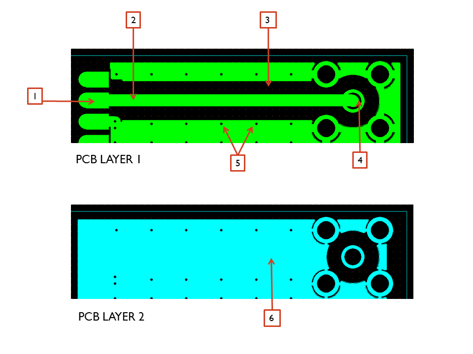
The following figure shows a layout example of a microstrip connecting an RF pad module to a through-hole RPSMA RF connector.
We do not recommend using a trace wider than the pad width, and using a very narrow trace can cause unwanted RF loss. You can minimize the length of the trace by placing the RPSMA jack close to the module. All of the grounds on the jack and the module are connected to the ground planes directly or through closely placed vias. Space any ground fill on the top layer at least twice the distance d (in this case, at least 0.050 in) from the microstrip to minimize their interaction.
| Number | Description |
|---|---|
| 1 |
XBee |
| 2 | 50 Ω microstrip trace |
| 3 | Back off ground fill at least twice the distance between layers 1 and 2 |
| 4 | RF connector |
| 5 | Stitch vias near the edges of the ground plane |
| 6 | Pour a solid ground plane under the RF trace on the reference layer |
Implementing these design suggestions helps ensure that the RF pad device performs to specifications.