Introduction
Purpose and Scope
The purpose of this document is to specify how to use SPI on XBee. As of the date of this writing, SPI is available on the following XBee radios:
- 2.4Ghz:
- XBee ZigBee S2C
- XBee3 Zigbee
- XBee3 802.15.4
- XBee3 Digimesh
- Wi-Fi:
- 868Mhz:
- XBee 868LP/865LP
- XBee SX 868
- 900Mhz:
- Cellular:
- XBee Cellular 3G
- XBee Cellular LTE Cat 1
- XBee3 Cellular LTE Cat 1
- XBee3 Cellular LTE-M/NB-IOT
Most aspects of SPI operate the same across product lines except where specified.
Conventions
Underbars in signal names are used to separate words. When a signal name is preceded by a lowercase ‘n’, that signal is asserted low (0 Volts).
Definition of Terms
Assert – Apply a voltage level to match its name. For example to assert Sleep_Rq means to request the module to sleep.
BPS – Bits per Second (where Kbps means 1000 bits per second, and Mbps means 1,000,000 bits per second).
OTA – Over the Air, i.e., using RF communications
Negate – Apply a signal to match the opposite of its name. For example, to negate Sleep_Rq means to request the module not to sleep or wake up.
Serial – Data is transmitted and received one bit at a time. Contrast serial with parallel, which sends multiple bits simultaneously using multiple data lines. Note that a serial interface typically implies an asynchronous interface. However, in the context of this document, serial means one bit at a time and is used to refer to either the asynchronous UART interface or the synchronous SPI interface.
Operation
This section specifies how SPI is implemented on the XBEE, what the SPI signals are, and how full-duplex operations work.
XBee Implementation of SPI
XBee modules will operate as an SPI slave only. An external master will provide the clock driving when data is sent and received. The maximum SPI clock rate for each supported XBee product is listed below:
- 3.5 Mbps
- XBee S6
- XBee 868LP/865LP
- XBee 900HP
- 5 Mbps
- XBee ZigBee S2C
- XBee3 Zigbee
- XBee3 802.15.4
- XBee3 Digimesh
- XBee S6B
- 6 Mbps
- XBee SX 868
- XBee SX 900
- XBee Cellular 3G
- XBee Cellular LTE Cat 1
- XBee3 Cellular LTE Cat 1
- XBee3 Cellular LTE-M/NB-IOT
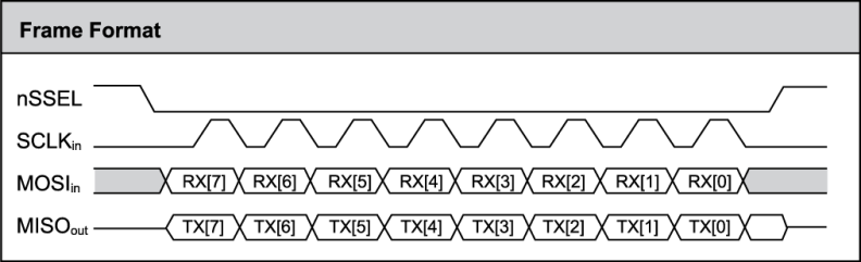
Data is transmitted and received with the most significant bit first (MSB first.) The radios use SPI mode 0, meaning the Clock Polarity (CPOL) and Clock Phase (CPHA) are both 0.
SPI Signals
The table below names the SPI signals and specifies their pinouts on the through-hole and surface mount modules. It also describes the operation of each pin:
Signal Name
dddddddddddddddd |
Signal Direction |
Through-hole pin and applicable AT command |
SMT pin and applicable AT command |
Description |
SPI_MOSI
(Master Out / Slave In) |
Input to XBee |
Pin 11, ATD4 |
Pin 16, ATP6 |
The SPI master outputs data on this line at the SPI_Clk rate after it selects the desired slave. When the SPI slave (XBee module) is configured for SPI operations, this pin is expected to be an input. |
SPI_MISO
(Master In / Slave Out) |
Output from XBee |
Pin 4, ATP2 |
Pin 17, ATP5 |
When SPI_nSSel is asserted (low) and SPI_Clk is active, the module outputs the data on this line at the SPI_Clk rate. When SPI_nSSel is negated (high), this output should be tri-stated such that another slave device can drive the line.
XBee S2C: The tri-stating of this line is not supported on S2C, and therefore other slaves cannot be connected to the same SPI bus. |
SPI_nSSel
(Slave Select) |
Input to XBee |
Pin 17, ATD3 |
Pin 15, ATP7 |
The SPI master outputs a low signal on this line to select the desired slave. When the SPI slave (XBee module) is configured for SPI operations, this pin is expected to be an input with an internal pull-up resistor. Be sure not to configure a pull-down resistor on this pin because it will prevent the SPI from working properly. |
SPI_Clk
(Clock) |
Input to XBee |
Pin 18, ATD2 |
Pin 14, ATP8 |
The SPI master outputs a clock on this pin, whose rate must not exceed the maximum supported by the XBee module. (See the table under XBee Implementation of SPI for the applicable maximum clock rate.) When the SPI slave (XBee module) is configured for SPI operations, this pin is expected to be an input. |
SPI_nATTN
(Attention) |
Output from XBee |
Pin 19, ATD1 |
Pin 12, ATP9 |
The SPI slave (XBee module) asserts this pin low whenever it has data to send to the master. After all data has been sent to the master, the SPI slave negates the pin (high). When this pin is configured for SPI operations, it is configured as an output. It is intended to signal the SPI master to assert SPI_nSSel and start SPI_Clk so that it can receive the data the XBee module has to send. |
Full Duplex Operation
The specification for SPI includes the four signals SPI_MISO, SPI_MOSI, SPi_Clk, and SPI_nSSel. However, using only these four signals, the SPI master cannot know when the slave device needs to send data. Therefore, the SPI slave cannot transmit unless enabled by the master. For this reason, we have made a SPI_nATTN signal available. This pin lets the XBee alert the SPI master that it has data to send.
SPI data is latched by the master and slave using the SPI_Clk signal. When data is being transferred, the MISO and MOSI signals change between each clock. If data is not available, then these signals will either not change staying at its previous value (0 or 1, ) or will always default to 0 depending on the model of XBee. This will result in receiving either a repetitive 0 or 0xFF. The means of determining whether or not received data is valid is by packetizing the data with API packets without escaping. Valid data to and from the XBee is delimited by 0x7E, a length, the payload, and finally a checksum byte. All other bytes read in both directions should be ignored. The bytes received between frames will be either 0xff or 0x00. This allows the SPI master to scan for a 0x7E delimiter between frames.
SPI allows for valid data from the slave to begin before, at the same time, or after valid data begins from the master. The interesting case is when the master is sending data to the slave and the slave has valid data to send in the middle of receiving data from the master. This allows a true full duplex operation where data is valid in both directions for a period of time. During this time, the master and slave must simultaneously transmit valid data at the clock speed so that no invalid bytes appear within an API frame, causing the whole frame to be discarded.
An example follows to more fully illustrate the SPI interface during the time valid data is being sent in both directions. First, the master asserts SPI_nSSel and starts SPI_Clk to send a frame to the slave. Initially, the slave doesn’t have valid data to send the master. However, while it is still receiving data from the master, it has its own data to send. Therefore, it asserts SPI_ nATTN low. Seeing that SPI_nSSel is already asserted and that SPI_Clk is active, it immediately begins sending valid data, even while it is receiving valid data from the master. In this example, the master finishes its valid data before the slave does. The master will have two indications of valid data: The SPI_nAttn line is asserted and the API frame length is not yet expired. For both of these reasons, the master should keep SPI_nSSel asserted and should keep SPI_Clk toggling in order to receive the end of the frame from the slave, even though these signals were originally turned on by the master to send data. During the time that the SPI master is sending invalid data to the SPI slave, it is important no 0x7E is included in that invalid data because that would trigger the SPI slave to start receiving another valid frame.
Low Power Operation
In general, sleep modes work the same on SPI as they do on UART. Describing all the various sleep modes is beyond the scope of this document. However, due to the addition of SPI mode, there is an option of another sleep pin, as described below:
By default, DIO8 (Sleep_Rq) is configured as a peripheral and is used for pin sleep to awaken and to sleep the module. This applies regardless of the selected serial interface (UART or SPI).
However, if Sleep_Rq is not configured as a peripheral and SPI_nSSel is configured as a peripheral, then pin sleep is controlled by SPI_nSSel rather than by Sleep_Rq. Asserting SPI_nSSel by driving it low either awakens the module or keeps it awake. Negating SPI_nSSel by driving it high puts the module to sleep.
Using SPI_nSSel for two purposes (to control sleep and to indicate that the SPI master has selected a particular slave device) has the advantage of requiring one less physical pin connection to implement pin sleep on SPI. It has the disadvantage of putting the module to sleep whenever the SPI master negates SPI_nSSel, even if that wasn’t the intent. (When using deep sleep, wakeup time from an unintended sleep may not be acceptable.) Therefore, if the user has full control of SPI_nSSel so that it can control pin sleep, whether or not data needs to be transmitted, then sharing the pin may be a good option in order to make the Sleep_Rq pin available for another purpose. Obviously, if the module is one of multiple slaves on the SPI, then the module would sleep while the SPI master talks to the other slave, but this is probably acceptable in most cases.
If neither pin is configured as a peripheral, then the module stays awake, being unable to sleep in SM1 mode.
Configuration
The three considerations for SPI configuration are:
- How is the serial port selected? (I.e. Should the UART or the SPI port be used?)
- If the SPI port is used, what should be the format of the data in order to avoid processing invalid characters while transmitting?
- What SPI options need to be configured?
Serial Port Selection
To enable the UART port, DIN (DIO14) and DOUT (DIO13) must be configured as peripherals. To enable the SPI port, SPI_MISO, SPI_MOSI, SPI_nSSel, and SPI_Clk must be enabled as peripherals. If both ports are enabled then output will go to the UART until the first input. Other rules for serial port selection are platform specific as follows:
Serial Port Selection on S2C
For the S2C, in the default configuration, the UART and the SPI ports will both be configured for serial I/O. However, input and output will use the UART as long as there is no SPI input. When the first SPI input happens, all subsequent I/O will use the SPI and the UART will not be usable without resetting the module.
If the configuration is changed so that only one port is configured, then that port will be the only one enabled or used immediately after reset for both input and output.
If neither serial port is enabled, the module will not support serial operations and all communications must be done OTA.
Serial Port Selection on SMT XBee radios that support SPI
In the default configuration, the UART and the SPI ports will both be configured for I/O. Initially, all serial data will go out the UART. But, as soon as input occurs on either port, that port is selected as the active port and no input or output will be allowed on the other port until the next reset of the module.
If the configuration is changed so that only one port is configured, then that port will be the only one enabled or used. If the parameters are written with only one port enabled, then the port that is not enabled will not even be used temporarily after the next reset.
SMT SPI works the same as S2C SPI with two minor variations:
- The first UART input selects the UART. (On the S2C, the SPI may still be used after the first UART input, but the UART may not be used after the first SPI input.)
- If both UART and SPI are disabled, then UART will be used. (On S2C, all serial I/O will be disabled.)
If both ports are disabled on reset, the UART will be used in spite of the wrong configuration so that at least one serial port will be operational for the module.
Serial Port Selection on through hole XBee radios that support SPI
In the default configuration, only the UART is configured for I/O. In order to use the SPI in a module using the default configuration, the user needs to hold DOUT low at the time the module is powered up or brought out of reset. This forces a configuration override of the SPI port so that it will be used rather than the UART. If the WR command is then issued through the SPI interface, DOUT will not need to be held low on the next module reset to force operation in SPI mode.
Since the SPI_nATTN line is critical for indicating that the SPI master needs to read, it will also be enabled when the other SPI lines are forced by holding down DOUT at reset, providing it was configured as disabled, which is the default configuration. When D1 (SPI_nATTN) is configured as a peripheral, its high to low transition indicates to the SPI master that the SPI slave is initialized and ready for data.
Thereafter, operation is like the SMT XBee radios:
- If both ports are enabled, then first input determines the serial port to use.
- If one port is enabled, then the enabled port is used.
- If neither port is enabled, then the UART is used in spite of the configuration.
Forcing UART operation
In the rare case that a module has been configured with only the SPI enabled and no SPI master is available to access the SPI slave port, the module may be recovered to UART operation by holding DIN low at reset time. As always, DIN forces a default configuration on the UART at 9600 baud and it will bring up the module in command mode on the UART port. Appropriate commands can then be sent to the module to configure it for UART operation. If those parameters are written, then the module will come up with the UART enabled, as desired on the next reset.
Data Format
The SPI will only operate in API mode with escaping disabled (AP=1). Transparent mode is not supported. This means that the AP configuration only applies to the UART and will be ignored while using SPI. The reason for this operation choice is that SPI is full duplex. If data flows in one direction, it flows in the other. Since it is not always possible to have valid data flowing in both directions at the same time, the receiver must have a way to parse out the valid data and to ignore the invalid data.
Officially, the invalid data is undefined for SPI. The only requirement is that the start of frame byte (0x7E) cannot be included in the invalid data as this would cause the receiver to begin parsing a new frame. But practically, the current XBee radios will always send ones or zeros as invalid data. Ignoring data without a header and checksum is still important to prevent problems from parsing partial frames.
SPI Options
Most host processors with SPI hardware allow the bit order, clock phase and polarity to be set. For communication with all XBee modules the host processor must set these options as follows:
- Bit Order: Send MSB first
- Clock Phase (CPHA): Sample data on first (leading) edge
- Clock Polarity (CPOL): First (leading) edge rises
This is SPI Mode 0 and MSB first for all XBee modules. Mode 0 means that data is sampled on the leading edge and that the leading edge rises. MSB first means that bit 7 is the first bit of a byte sent over the interface.
Last updated:
Jan 01, 2024